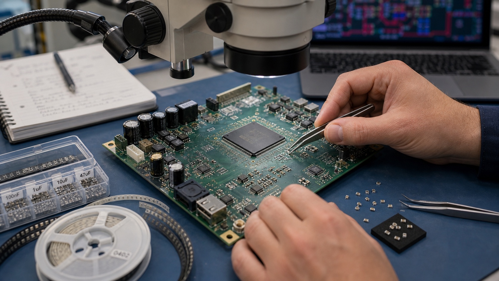
The hundred-nanofarad reflex
Open almost any reference schematic and you will find a 100 nF capacitor parked next to every power pin, copied verbatim into the next design and the one after that. It is a reflex, not a decision. The actual job of decoupling is narrower and more interesting: hold the power rail’s impedance below some target value across the whole band of frequencies at which your chips yank current out of it. Whether you need one cap, six caps, or a buried plane pair is an answer you read off an impedance-versus-frequency curve — not a number you inherit from cargo-cult.
What decoupling actually does
A digital IC does not draw current smoothly. Every clock edge switches millions of gates, and each switching event pulls a slug of charge to flip its load capacitance. That demand arrives as di/dt — current that changes fast. The regulator feeding the rail is hopelessly slow by comparison: a typical buck converter’s control loop has a bandwidth of maybe 50–200 kHz, so above that it simply cannot respond. For anything faster, the charge has to come from somewhere local. That somewhere is your decoupling capacitors.
A capacitor near the pin acts as a tiny local reservoir. When the chip demands a burst, the cap dumps charge; between bursts, the regulator trickles it back up. If the reservoir is too small, too far, or too slow, the rail voltage sags during the transient. Sag is not cosmetic: it shrinks timing margins, raises jitter, trips brown-out detectors, and radiates the resulting ripple as EMI. Decoupling is impedance management in disguise — you are keeping the rail stiff so that a fast current swing produces only a small voltage swing.
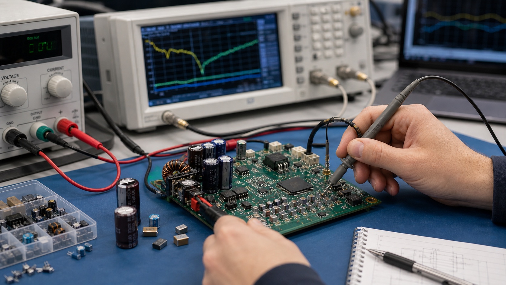
The impedance-versus-frequency view
Ohm’s law for an AC rail is ΔV = ΔI × Z. The voltage wobble the chip sees equals the current it pulls times the impedance looking back into the power distribution network (PDN) at that frequency. Flip it around and you get the design target every PDN problem reduces to:
Ztarget = ΔV / ΔI
Pick the worst-case transient current and the ripple you can tolerate, divide, and you have the impedance ceiling the network must stay under from DC up to the highest frequency the load excites. Decoupling caps are simply the parts that pull the curve down where the regulator and the planes cannot.
Worked example. A 3.3 V rail, 5% ripple budget, feeding a load that can swing 2 A in a few nanoseconds:
- ΔV = 5% × 3.3 V = 0.165 V (165 mV)
- ΔI = 2 A
- Ztarget = 0.165 V ÷ 2 A = 0.0825 Ω ≈ 82.5 mΩ
So the entire PDN — regulator output, bulk caps, bypass caps, planes, vias — must present under ~83 mΩ across the band, perhaps from a few kilohertz to a few hundred megahertz. That single number reframes the whole job: you are not “adding decoupling,” you are filling in the parts of the impedance curve that poke above 83 mΩ. Tighten the ripple spec to 2% and the ceiling drops to ~33 mΩ and the part count climbs. (For a fast core rail a vendor will often quote a tighter target still; the method is identical, only the number moves.)
A real cap is an RLC, not a C
The reason one capacitor cannot do the whole job is that a real capacitor stops behaving like a capacitor partway up the band. Its impedance is the series combination of three things:
- Capacitance (C) — impedance falls with frequency: ZC = 1 / (2πfC). This is the regime you want.
- ESR (equivalent series resistance) — a flat resistive floor at the bottom of the curve, the lowest impedance the part can reach.
- ESL (equivalent series inductance) — impedance rises with frequency: ZL = 2πfL. This comes from the cap’s internal geometry plus, critically, the pads, vias and traces connecting it.
Capacitance dominates at low frequency, inductance at high frequency, and where they cross the impedance hits its minimum (just the ESR). That crossover is the self-resonant frequency:
fSRF = 1 / (2π√(LC))
Above fSRF the capacitor is inductive — its impedance climbs, and it is no longer decoupling anything. This is the punchline that kills the “100 nF on everything” habit.
Worked example. A 100 nF part in an 0402 package, with roughly 0.5 nH of total loop inductance (mount included):
- LC = 0.5 nH × 100 nF = (0.5 × 10−9) × (100 × 10−9) = 5 × 10⁻¹⁷
- √(LC) = 7.07 × 10⁻⁹
- fSRF = 1 ÷ (2π × 7.07 × 10−9) ≈ 22 MHz
Your beloved 100 nF is inductive above ~22 MHz. A chip with 1 ns edges has meaningful energy out past 300 MHz, where that 0.5 nH alone presents 2π × 300 MHz × 0.5 nH ≈ 0.94 Ω — more than ten times over our 83 mΩ budget. The value printed on the cap is irrelevant up there; the inductance of how you mounted it is everything. Run the same numbers on a 1 µF and fSRF drops to ~7 MHz; on a 10 µF (bigger package, ~1 nH) to ~1.6 MHz. Bigger value, lower resonance — which is exactly why you need a spread of values, each minding its own slice of the band.
The three tiers
Because each capacitor only covers a band around its fSRF, you stack parts of different values so their low-impedance regions overlap into one continuous low-impedance curve. Think of it as three tiers, each handing off to the next as frequency climbs:
- Bulk (low frequency, ~1 kHz–1 MHz). Tantalum, polymer, or aluminium-electrolytic in the tens-to-hundreds of microfarads. These are the deep reservoir that rides out big, relatively slow load steps and covers the gap between the regulator’s loop bandwidth and where the MLCCs take over. They have high ESL and are useless at RF — that is fine, it is not their job.
- Mid (~100 kHz–10 MHz). MLCCs of 1–10 µF (0603/0805). These bridge bulk and bypass and carry the bulk of the medium-speed transient charge.
- Bypass / high frequency (~10 MHz and up). Small MLCCs, 100 nF down to 1 nF, in 0402/0201, sitting right at the IC pins. Small value means low ESL and a high fSRF, so these are the only parts still working at the top of the band — provided you mount them tightly.
The goal is a smooth low-impedance trough across the whole range, not maximum total capacitance. A megafarad of bulk does nothing for a 200 MHz current spike.
Placement and loop inductance
Above roughly 100 MHz, the dominant inductance is no longer inside the capacitor — it is the loop the current travels: out of the cap, through its pad, down a via, across the plane, up another via to the IC pin, and back. That loop’s area sets its inductance, and inductance is what stands between the chip and its charge at high frequency. A sloppy mount can add a nanohenry or more, dwarfing the part’s own ESL. At 100 MHz an extra 1 nH is 2π × 100 MHz × 1 nH ≈ 0.63 Ω — on its own, almost eight times the budget. So:
- Put the smallest, fastest caps closest to the pins. Tier them outward by value — bypass hugging the pin, mid nearby, bulk allowed to live further out near the regulator.
- Minimize the loop: short, fat connections; place the cap as near as the footprint allows; drop the via right at the pad (via-in-pad on dense BGAs) rather than running a stub trace to a far via.
- Get the cap to its planes with the shortest, lowest-inductance vias you can — doubled vias per pad roughly halve that contribution, and a thin power-to-ground dielectric shortens the vertical loop.
- Which side of the board the cap sits on matters: mounting it on the back directly under the pin can beat a far-side neighbour, because the via loop is shorter than the lateral one.
Plane capacitance and the top of the band
At the very top of the band, discrete caps lose because their mounting inductance is too high — and here the PCB itself helps. A closely-spaced power/ground plane pair forms a parallel-plate capacitor that is small in value (often only a few nanofarads on a typical board) but has near-zero inductance and is distributed everywhere at once. That makes it the best high-frequency decoupling you have above a few hundred megahertz, exactly where MLCCs have gone inductive. You buy it with stackup, not parts: keep power and ground on adjacent layers with a thin dielectric between them. On a fast design this plane capacitance is not a bonus — it is load-bearing, and a stackup that separates power from its return ground by several layers throws it away.
Anti-resonance: why more caps can be worse
Here is the trap that surprises people. When you parallel two different values, you get a parallel-resonant tank between them: above the larger cap’s fSRF it looks inductive, while the smaller cap is still capacitive, and an inductor in parallel with a capacitor resonates. At that anti-resonant frequency the two impedances cancel and the parallel combination spikes upward — an impedance peak sitting in the band you were trying to flatten, possibly poking back above Ztarget. Adding a cap made one frequency worse.
This is why “throw more caps at it” is not a strategy and why a wall of one value is no better. Practical defences:
- Do not space values by huge ratios. Steps of roughly 10× (10 µF / 1 µF / 100 nF) keep peaks low and in the noise; jumping 10 µF straight to 1 nF leaves a tall peak between them.
- Lean on ESR for damping. A little series resistance flattens the peak. This is the dirty secret of why an all-MLCC, ultra-low-ESR rail can ring while a design with one modest-ESR bulk cap stays calm — the lossy part damps the tank.
- Favour fewer values in quantity over a museum of distinct values. Several 100 nF parts in parallel push the band down without creating new resonances between each other (same fSRF, so they just lower the floor); a zoo of mismatched values manufactures peaks.
Per-rail bulk vs per-pin bypass
Two different questions hide inside “how many caps,” and they have different answers.
Per-rail bulk is about total energy and the low-frequency droop on a whole supply. Size it from the transient: each rail wants enough bulk near its regulator to ride the largest load step within the ripple budget, plus a mid-tier cap or two to bridge to the bypass band. A rail feeding a switching converter or a motor driver needs healthy bulk close to the switch node and the input pins — skimp here and the switcher’s own di/dt collapses its input rail and sprays conducted EMI. A quiet, slow housekeeping rail may be content with a single bulk cap and a couple of bypasses.
Per-pin bypass is about local high-frequency demand at each power pin. The honest rule is per-pin by current and edge rate, not religiously one-per-pin. A fast BGA with dozens of core and I/O power balls genuinely needs a dense field of small caps fanned out underneath — the loop to a pin on the far side is too long to share. A small jellybean part toggling slowly is fine with one bypass shared across a couple of nearby pins. Always start from the datasheet: many MCU and SoC vendors specify exactly which pins want which value, and that guidance reflects the die’s internal power domains. Follow it — then sanity-check it against your Ztarget, because a reference design tuned for a different ripple spec than yours is still cargo-cult if you copy it blind.
Common mistakes and failure modes
- 100 nF everywhere, no bulk. The classic. Plenty of high-frequency bypass and nothing to source a 1 A load step — the rail droops on every burst and the regulator hunts. A field of identical small caps cannot supply low-frequency energy.
- Caps placed far from the pins. A perfect value with a long, skinny trace to a distant via is inductance in series with your reservoir. Above ~100 MHz the mount, not the value, decides whether the cap works at all.
- All-identical values causing nothing — or a zoo causing anti-resonance. One value covers one band; a badly-spread set builds impedance peaks between values. Both extremes leave holes in the curve.
- Ignoring ESL and the mount. Treating a 100 nF as a 100 nF at 300 MHz. At RF it is a small inductor, full stop.
- No bulk near a switcher. Input and switch-node decoupling missing or far away — instant conducted-EMI failure and a noisy input rail that pollutes everything upstream.
- Oversizing values that do nothing. Swapping a 100 nF for a 10 µF at the pin to “be safe.” The bigger part has a lower fSRF and is inductive sooner — worse at exactly the high frequencies the pin cares about.
- DC-bias derating ignored. A small high-K MLCC (X5R/X7R 0402) can lose 50–80% of its marked capacitance at its rated voltage. Your “10 µF” may be acting like 3 µF on a 3.3 V rail. Read the bias curve, not the marking.
The practical checklist
| Tier | Typical value & package | Role / band | Placement |
|---|---|---|---|
| Bulk | 22–470 µF tantalum / polymer / electrolytic | Energy reservoir, ~1 kHz–1 MHz; rides big load steps | Near the regulator output; one per rail (more on high-current rails) |
| Mid | 1–10 µF MLCC (0603/0805) | Bridges bulk to bypass, ~100 kHz–10 MHz | Between regulator and IC; a few distributed near the load |
| Bypass | 100 nF–1 nF MLCC (0402/0201) | High-frequency local charge, ~10 MHz and up | Right at the power pins; shortest possible loop, via at the pad |
| Plane pair | Distributed (a few nF), thin dielectric | Top-of-band, hundreds of MHz; lowest inductance | Adjacent power/ground layers in the stackup |
- Compute Ztarget = ΔV / ΔI for each rail before placing a single cap.
- Start from the chip datasheet’s decoupling table; treat it as a floor, not gospel.
- Bulk near every regulator; extra bulk and tight input decoupling on switchers and drivers.
- Bypass density set by pin current and edge rate — dense under BGAs, sparse on slow parts.
- Space values ~10× apart; prefer quantity of a few values over a zoo of many.
- Minimize every loop: cap close, via in/at the pad, doubled vias, thin power-to-ground dielectric.
- Derate MLCCs for DC bias — verify effective, not marked, capacitance.
- On fast designs, simulate the PDN impedance curve and confirm it stays under Ztarget with no anti-resonant peaks poking through.
Decoupling is not a sprinkle of identical caps — it is keeping the rail’s impedance below ΔV÷ΔI across every frequency your chips pull current, which takes a deliberate spread of values, mounted tight, not a reflexive 100 nF on every pin.