What a pre-screen actually is
It is not a pass certificate. A pre-screen is a few hundred dollars of bench time — a near-field probe and a spectrum analyzer, or a half-day in a pre-compliance chamber — to find the 3–6 dB problems while they are still cheap to fix. You are looking for where you sit close to the radiated-emissions limit and why, not collecting a stamp. The full-compliance test at an accredited lab answers one question: pass or fail. The pre-screen answers the question that actually saves you money — which feature on which axis is the problem, and is it a slot, a cable, or a clock?
Think of it as the EMC equivalent of a dry-fit before you glue. You run it precisely because the cost of being wrong has not yet been baked into steel. A two-hour session that tells you the display flex is the dominant radiator at 600 MHz is worth more, at the right moment, than a perfect ±0.5 dB compliance report that arrives after the tool is cut.
The bench setup, concretely
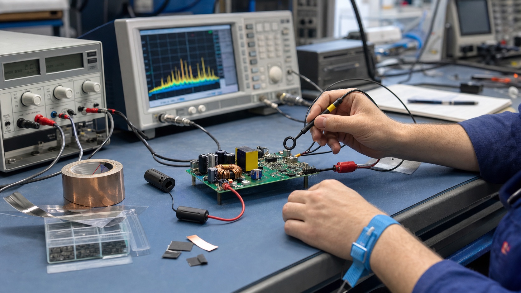
A useful pre-screen is not one instrument; it is a small stack, run in layers from cheapest to most representative. You do not need all of it on day one, but you should know what each layer tells you.
- Near-field probes (the diagnostic workhorse). A set of H-field loops and an E-field stub, a wideband amplifier, and a spectrum analyzer. These do not measure compliance — they have no calibrated distance — but they tell you where the energy lives. Float the loop a few millimetres over the switcher, the clock oscillator, each connector, and each seam, and watch which peak moves. This is how you assign blame to a specific component or aperture in minutes.
- LISN and conducted setup. A line-impedance stabilization network in series with mains (or the DC input) presents a defined 50 Ω impedance and lets the analyzer see what your product is pushing back onto its power leads from roughly 150 kHz to 30 MHz. This is where switching-supply noise and common-mode currents on the cable show up first.
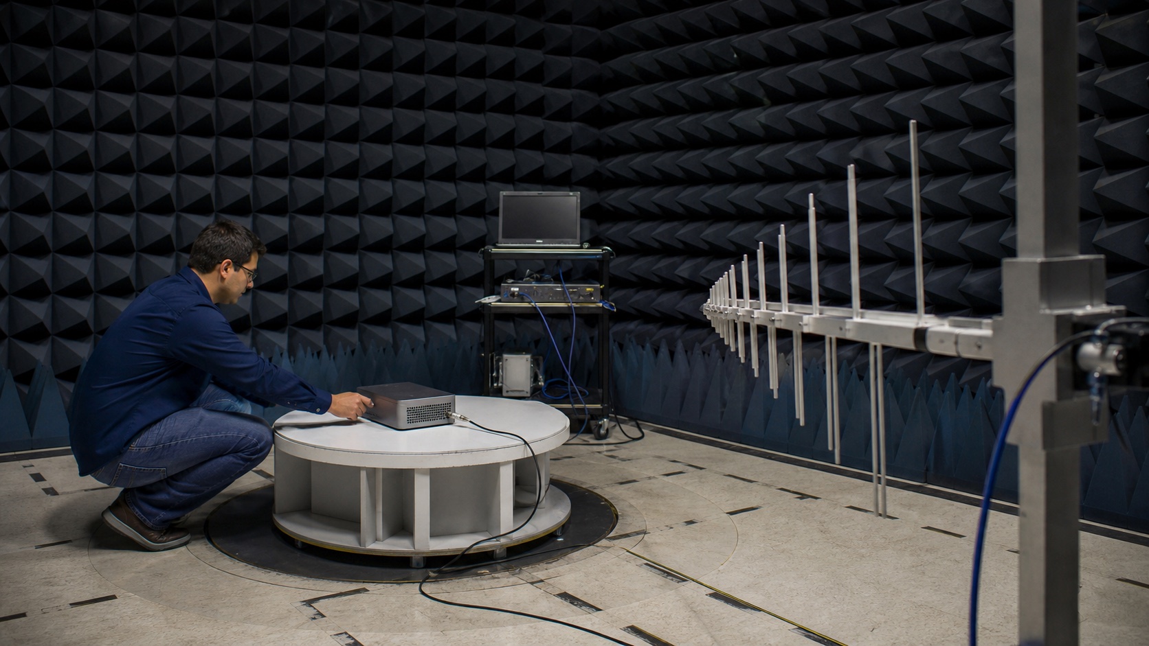
- Antenna plus analyzer (radiated). A broadband antenna — a biconical/log-periodic combo or a simple wideband horn — at a fixed distance, feeding the analyzer set to peak-hold. Even in a noisy lab (not a chamber) you can sweep, rotate the unit on a turntable, and find your worst azimuth. The absolute numbers are contaminated by ambient FM, cellular, and Wi-Fi, but the shape of your emission profile is real.
- A pre-compliance chamber, half a day. When you want numbers you can trust to within a few dB, you book a semi-anechoic chamber or a compact GTEM/TEM cell for an afternoon. This strips out the ambient and gives you a calibrated distance, so a peak that reads 6 dB under the limit on your bench can be confirmed as a real 3 dB margin — or exposed as a 2 dB exceedance you would otherwise have shipped.
The order matters. Probes find the culprit, the LISN and antenna tell you whether it leaves the box, and the chamber half-day converts your hunches into margins. Run them in that sequence and a single engineer can characterize a product in a day.
Why mechanical geometry dominates EMI
Here is the physics that makes housing-lock the real deadline: at the frequencies that fail compliance, your enclosure and cables are antennas, and antennas are defined by geometry. The radiating structure is almost never the silicon — it is the copper, the seams, and the wires that the silicon drives. Change the geometry and you change the antenna; change the firmware and you mostly change how hard you drive it.
Four geometric mechanisms account for the bulk of what you will see:
- Slots and apertures as antennas. Any gap in a conductive shield — a seam between two housing halves, a display window, a speaker grille, an unscreened vent — radiates most efficiently when its longest dimension approaches a half-wavelength. A slot leaks like a dipole rotated 90°; its long edge, not its area, sets the resonant frequency. A 1 mm-tall, 100 mm-long seam is a far better antenna than a 20 mm round hole.
- Ground stitching and the return path. Every fast signal needs a low-impedance return directly beneath it. Stitching vias tie reference planes together and keep that return tight; a starved or split plane forces the return current to detour, and the loop it carves out becomes a magnetic-loop antenna. The current does not care about your schematic — above a few megahertz it follows the path of least inductance, which is the copper directly under the trace.
- Cable bonding. A cable is the longest conductor in most products, so it is the most efficient antenna you own. What matters is how its shield (or its 0 V reference) bonds to chassis at the point of entry. A 360° bond drains common-mode current to ground; a thin “pigtail” wire to a single pin is an inductor that turns the whole cable into a transmitting whip.
- Gasket and shield-can placement. Conductive gaskets, board-level shield cans, and finger-stock all exist to keep aperture lengths short and ground continuous across a joint. Where they go — and whether the housing has the bosses, lips, and contact surfaces to seat them — is decided in CAD, long before anyone powers the board.
Notice that all four are mechanical decisions. That is the whole argument for the timing: roughly 80% of an EMI fix is geometry — aperture size, gasket seat, stitch pitch, cable entry — and only about 20% is electrical (a snubber, a common-mode choke, a slower edge). Before tooling, both levers are free. After tooling, only the expensive 20% remains.
The usual culprits, and roughly where they sit
Emissions are not random; the same handful of sources show up across most products, each with a characteristic frequency signature. Knowing the signature lets you read the analyzer like a map.
- Switching regulators and their harmonics. A DC-DC converter switching at 500 kHz–2 MHz produces a comb of harmonics that, thanks to fast switch-node edges, extends well past 100 MHz. These dominate the conducted band (150 kHz–30 MHz) and often seed the lower radiated band. The energy is in the edge, not the fundamental — a 1 ns transition has meaningful content out beyond 300 MHz.
- Fast digital clocks and their edges. Crystal oscillators, processor clocks, DDR, and high-speed serial links radiate at their fundamental and at every odd-and-even harmonic. A clock with a 1 ns edge has a spectral “knee” near 1/(π×tr) ≈ 300 MHz, above which harmonics start rolling off — but the early harmonics, in the 200 MHz–1 GHz range, are exactly where Class B limits are tightest.
- Display flex cables. The ribbon between the main board and an LCD/OLED carries fast pixel-clock and data lines, often with marginal ground return, and it is physically long and mobile. It is one of the most common dominant radiators in consumer products, typically misbehaving somewhere in the 300 MHz–1 GHz window.
- DC motors and brush noise. Brushed motors arc at the commutator, producing broadband impulsive noise from tens of kHz up into the hundreds of MHz. It is wideband hash rather than a clean tone, and it couples straight onto the motor leads — which then radiate. This is a conducted and radiated problem at once.
Two of these — switchers and motors — live mostly in the conducted world; two — clocks and display flex — live mostly in the radiated world; and the regulator straddles both. That split maps directly onto your bench layers.
Radiated versus conducted — two problems, two fixes
It is worth being explicit, because the fixes do not transfer. Conducted emissions are the RF currents your product injects back onto its power and signal cables, measured against the LISN, broadly 150 kHz–30 MHz. You fix them at the source and the port: input filtering, common-mode chokes, Y-capacitors, a clean return, and a good chassis bond where the cable enters. Radiated emissions are the fields the product launches into space, measured with an antenna, broadly 30 MHz–1 GHz and up (6 GHz+ for products with fast digital or high-frequency radios). You fix those with geometry: shorter apertures, tighter stitching, shield cans, gaskets, and controlled cable lengths.
The trap is that they share root causes. A poorly bonded cable shows up as conducted noise at 10 MHz and as a radiated peak at 300 MHz, because the same common-mode current that flows back onto the line also drives the cable as an antenna. Fix the bond once, mechanically, and both numbers improve. That dual payoff is exactly the kind of thing a pre-screen surfaces while you can still act on it.
ESD and the housing
Emissions are not the only thing the enclosure decides. Electrostatic discharge — the ±4 to ±15 kV contact and air-discharge events of IEC 61000-4-2 — is overwhelmingly a mechanical problem. Where can an 8 kV arc reach? Every seam, button, connector shell, screw head, and display edge is a candidate entry point. The defense is geometry: creepage distance from exposed metal to sensitive nets, a deliberate path that steers the discharge to chassis rather than through your microcontroller, and the decision of whether a port shell bonds to ground or floats.
You cannot add creepage, move a button stack, or change which metal is user-accessible after the tool is cut — not without new steel. So ESD survivability belongs on the same pre-lock checklist as emissions: it is the same housing, decided at the same moment, governed by the same physics of where conductors sit relative to each other.
A worked example: the seam that fails at 1.5 GHz
Suppose your product has a 100 mm-long seam where two housing halves meet, and you are relying on press-fit plastic with no gasket and no continuous ground across the joint. Treat the seam as a slot antenna. Its resonant frequency is roughly where the slot length equals a half-wavelength:
f ≈ c ÷ (2 × L) = (3 × 10⁸ m/s) ÷ (2 × 0.100 m) ≈ 1.5 GHz.
Now bring in the source. Say the board runs a 25 MHz system clock. Its harmonics fall at 25, 50, 75 MHz… and the 60th harmonic sits at exactly 1.5 GHz — right where your seam radiates most efficiently. You have unintentionally built a tuned transmitter: a source delivering energy to a slot that is resonant at that very frequency. On the analyzer this looks like a sharp peak poking 4 dB above the limit line, and nothing in the firmware will move it, because the firmware is not the antenna.
The geometric fixes are all pre-tool and all cheap: shorten the effective slot by adding ground-contact points along the seam so no continuous gap exceeds, say, 25 mm (which pushes the resonance up to ~6 GHz, out of the troublesome band and onto a steeper part of the harmonic roll-off); add a conductive gasket lip; or design the parting line away from the noisy section entirely. Each of those is a CAD edit today. After tooling, your only moves are to attack the source — spread-spectrum the clock, slow the edge, add a board-level can — the expensive 20%, fighting physics instead of using it.
The margin framing is the punchline. A pre-screen that reads “+4 dB at 1.5 GHz, dominant aperture is the main seam” hands you a one-line CAD task. The same discovery at the compliance lab, at 90% tooling, hands you a respin-or-retool decision and a slipped launch.
Common mistakes and failure modes
The expensive failures are not exotic. They cluster around a few recurring errors, almost all of them committed in CAD and discovered at the lab.
- Grounding a shield at one end only. A cable shield or shield can bonded at a single point is an antenna, not a shield. Above a few MHz it needs a low-impedance bond at both ends (or a 360° bond at entry) to actually carry the common-mode current to ground rather than re-radiate it.
- The pigtail. Terminating a shield with a thin twisted wire to one pin adds series inductance that defeats the shield exactly where you need it. Plan for a circumferential bond at the connector or chassis entry.
- The unstitched seam. Two plated or coated housing halves that meet without continuous contact form a slot the full length of the joint. Conductive coating with no stitching across the parting line is theatre — the gap is still there electrically.
- Antenna next to the battery (or metal, or the hand). Placing the radio antenna against the battery, a metal bracket, a speaker magnet, or where the user’s grip lands detunes it and tanks efficiency. Now firmware turns up TX power to compensate — and emissions rise with it. Antenna keep-outs are mechanical, and they are not negotiable after tooling.
- Filtering at the wrong end of the cable. A common-mode choke or filter cap does its job only at the port where the noise enters or leaves. Put it 40 mm downstream of the connector and the stub between filter and port still radiates.
- Finding it at the FCC/CE test. The most expensive failure mode of all: treating compliance as the first measurement rather than the last. By then the enclosure is steel, the schedule is committed, and your remaining options are a respin, a tooling change, or a field bodge.
The pre-lock checklist
Run this before you commit the enclosure tooling. None of it needs the final firmware; all of it gets cheaper the earlier you do it.
| Check | What you are looking for |
|---|---|
| Near-field sweep of the board | Which component (switcher, clock, flex) is the dominant radiator, and on which net |
| Conducted scan on the LISN | Margin from 150 kHz–30 MHz; whether input filtering is sized right |
| Radiated sweep, unit rotated | Worst-case azimuth and the peaks closest to the limit, with their frequencies noted |
| Longest seam / aperture vs. half-wave | f ≈ c÷(2×L) for every gap; flag any landing near a known harmonic |
| Cable entries and shield bonds | 360° bonds, no pigtails, filtering seated at the port |
| Ground stitching and return paths | No split planes under fast edges; stitch pitch tight along board and housing seams |
| Antenna keep-out | Clearance from battery, metal, and the user’s hand confirmed in CAD |
| ESD entry points | Creepage from exposed metal to sensitive nets; a deliberate path to chassis |
| Gasket / shield-can seats | Bosses, lips, and contact surfaces present in the housing to seat them |
If every row is answered, you have spent an afternoon and you can lock the tool with confidence. If even one is a shrug, that shrug is cheaper to resolve now than at first article.
What it costs to skip it
A failed radiated-emissions test at 90% tooling leaves three bad options: a board respin (4–6 weeks and a new BOM), a tooling change (weeks of lead time and real money for a steel edit), or a ferrite-and-copper-tape field fix that adds labor to every single production unit and never fully closes the margin. Each one slips your launch and bruises your gross margin. The pre-screen that would have caught it was one afternoon and a few hundred dollars of bench time — spent while the fix was still a line in CAD instead of a change order on a mold.
EMI is decided by geometry, and geometry is free to change only until the tool is cut. Run the pre-screen before that window closes — not after the first article comes back from the lab.